Odanaka's work on TCAD(Technology Computer-Aided Design) †
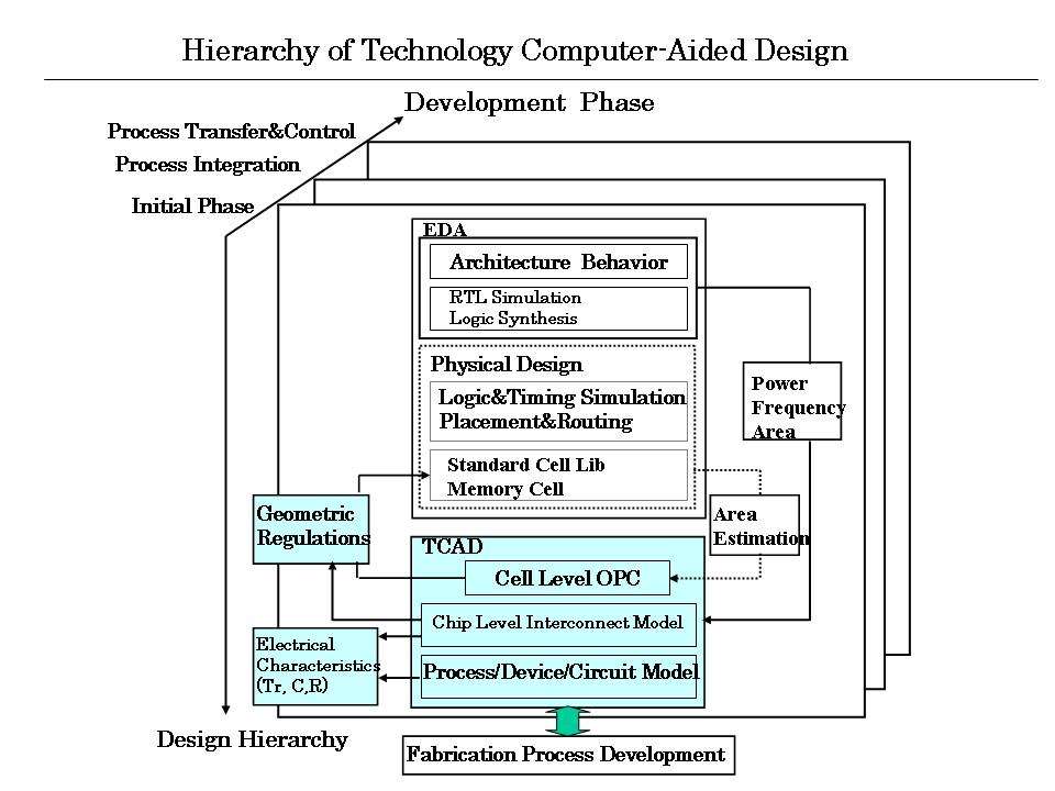
The numerical and mathematical models play an important role in the development of semiconductor simulations and computer-aided design for semiconductor integrated circuits processes and devices, which is called TCAD(Technology Computer-Aided Design) in semiconductor industry since the end of 1980s. We have made some contributions to create a technical area of TCAD, including a pioneer work of 3D multi-physics simulations on a supercomputer for IC processes and devices, numerical reliability simulations, and a wide variety of semiconductor device design. Recently, our numerical methods for solving QDD equations(QDD Model) are widely used in TCAD for advanced semiconductor devices such as double-gate MOSFETs and Si nanowire FETs, as well as statistical variability simulations of CMOS devices. TCAD consists of a heirarchy of multi-scale design models related to materials and fabrication processes, devices, interconnects, patterns, and circuits. In the practical use, the TCAD system is considered as a "dynamical" design system, which depends on the phase of fabrication process development. The future role of TCAD is to provide a "design platform", which overcomes unmanageable complexity between the new fabrication process development and integrated circuit design, as well as performance analysis and systematic design of new memory and logic devices with multi-scale and multi-physics simulations.

Design hierarchy in TCAD †
- S.Odanaka et al., "A design hierarchy of IC interconnects and gate patterns," IEICE Trans. Electron., vol.E82-C, pp.948-954, 1999.
 Oda99.pdf
Supercomputer-aided design †
- S. Odanaka et al., “SMART: Three-dimensional process/device
simulator integrated on a super-computer,” in ISCAS Proc., vol. 2,
pp. 534-537, 1987.
- S.Odanaka et al., "SMART-P: Rigorous three-dimensional process simulator on a supercomputer", IEEE Trans. Computer Aided Design of ICAS, vol.7, pp.675-683, 1988.
- S.Odanaka et al., "SMART-II:A three-dimensional CAD model for submicrometer MOSFET's," IEEE Trans. Computer Aided Design of ICAS, vol.10, pp.619-628,1991.
- S.Odanaka and T.Nogi, "Massivelly parallel computation using a splitting up operator method for three-dimensional device simulation," IEEE Trans. Computer Aided Design of ICAS, vol.14, pp.824-832, 1995.
 Oda95.pdf
Semiconductor device design †
- S.Odanaka et al., "A new half-micrometer p-channel MOSFET with efficient punchthrough stops," IEEE Trans. Electron Devices,vol.33, pp.317-321, 1986.
- S. Odanaka et al., "A self-aligned retrograde twin-well structure with buried p+-layer", IEEE Trans. on Electron Devices,vol.37, pp.1735-1742,1990.
- S.Odanaka and A.Hiroki, "Potential design and transport property of 0.1 um MOSFET with asymmetric channel profile," IEEE Trans. Electron Devices, vol.44, pp.595-600,1997.
 Oda97.pdf
- S.Odanaka et al., "Double Pocket Architecture Using Indium and Boron
for Sub-100 nm MOSFETs," IEEE Electron Devices Letters, vol.22, pp.330-332, 2001.
 Oda01.pdf
Understanding of physical phenomena †
- S.Odanaka et al., "The dynamics of latchup turn-on behavior in scaled CMOS," IEEE Trans. Electron Devices, vol.32, pp.1334-1340, 1985.
 Oda85.pdf
- S.Odanaka and A.Hiroki, "A numerical simulation of hot-carrier induced device degradation," in Proceedings of VPAD, pp.108-111,1991.
 Oda91.pdf
![[PukiWiki] [PukiWiki]](image/Fuji08.jpeg)
![[PukiWiki] [PukiWiki]](image/Fuji08.jpeg)